- 您现在的位置:买卖IC网 > Sheet目录39248 > LM3460M5X-1.5/NOPB (NATIONAL SEMICONDUCTOR CORP) 1-OUTPUT THREE TERM VOLTAGE REFERENCE, 1.5 V, PDSO5
Absolute Maximum Ratings (Note 1)
If Military/Aerospace specified devices are required,
please contact the National Semiconductor Sales Office/
Distributors for availability and specifications.
Input Voltage V
IN
20V
Output Current
20 mA
Junction Temperature
150C
Storage Temperature
65C to +150C
Lead Temperature
Vapor Phase (60 sec.)
Infared (15 sec.)
+215C
+220C
Power Dissipation (T
A = 25C)
300 mW
ESD Susceptibility (Note 3)
Human Body Model
1500V
See AN-450 "Surface Mounting Methods and Their Effect
on Product Reliability" for methods on soldering surface
mount devices.
Operating Ratings (Note 1), (Note 2)
Ambient Temperature Range
0C
≤ T
A
≤ +70C
Output Current
1 mA
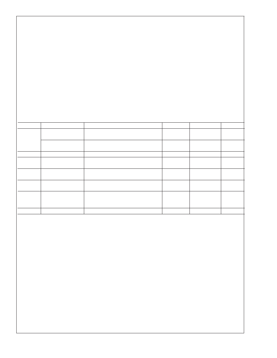
Electrical Characteristics
LM3460-1.5
Specifications with standard type face are for T
J = 25C, and those with boldface type apply over full Operating Tempera-
ture Range. Unless otherwise specified, (+)IN = V
REG,VOUT = 200 mV
Symbol
Parameter
Conditions
Typ (Note 4)
Limit (Note 5)
Units
V
REG
Regulated Voltage
I
OUT = 1 mA
1.5
1.515/ 1.530
1.485/1.470
V (max)
V (min)
Regulated Voltage
Tolerance
I
OUT =1mA
±1/ ±2
% (max)
I
q
Quiescent Current
I
OUT = 1 mA
85
125/150
A (max)
G
m
Transconductance
I
OUT /
V
REG
20A
≤ I
OUT
≤ 1mA
V
OUT = 500 mV
3.3
1/0.5
mA/mV
(min)
V
SAT
Output Saturation
V
IN =VREG + 100 mV
I
OUT =1mA
0.8
0.95
V (max)
I
L
Output Leakage
Current
V
IN =VREG 100 mV
V
OUT =0V
0.1
0.5/1.0
A (max)
R
F
Internal Feedback
Resistor (See
Functional Diagram)
7.1
8.9
5.3
k
(max)
k
(min)
E
n
Output Noise Voltage
I
OUT = 1 mA, 10 Hz
≤ f ≤ 10kHz
50
V (rms)
LM3460
www.national.com
3
发布紧急采购,3分钟左右您将得到回复。
相关PDF资料
LM3670MFX-2.5/NOPB
0.75 A SWITCHING REGULATOR, 1300 kHz SWITCHING FREQ-MAX, PDSO5
LM368H-6.2
1-OUTPUT TWO TERM VOLTAGE REFERENCE, 6.2 V, MBCY8
LM368YH-6.2
1-OUTPUT TWO TERM VOLTAGE REFERENCE, 6.2 V, MBCY8
LM385AXM-2.5X
1-OUTPUT TWO TERM VOLTAGE REFERENCE, 2.5 V, PDSO8
LM285AM-2.5X
1-OUTPUT TWO TERM VOLTAGE REFERENCE, 2.5 V, PDSO8
LM385AYM-2.5X
1-OUTPUT TWO TERM VOLTAGE REFERENCE, 2.5 V, PDSO8
LM385AM-2.5X
1-OUTPUT TWO TERM VOLTAGE REFERENCE, 2.5 V, PDSO8
LM385D-2.5R2
1-OUTPUT TWO TERM VOLTAGE REFERENCE, 2.5 V, PDSO8
相关代理商/技术参数
LM3460M5X15
制造商:Texas Instruments 功能描述:*
LM3463
制造商:TI 制造商全称:Texas Instruments 功能描述:Dynamic Headroom Controller with Thermal Control Interface and Individual Channel Dimming Control
LM3463_12
制造商:TI 制造商全称:Texas Instruments 功能描述:LM3463 Dynamic Headroom Controller with Thermal Control Interface and Individual Channel Dimming Control
LM3463EVM
功能描述:LED 照明开发工具 LM3463EVM Eval Mod RoHS:否 制造商:Fairchild Semiconductor 产品:Evaluation Kits 用于:FL7732 核心: 电源电压:120V 系列: 封装:
LM3463EVM
制造商:Texas Instruments 功能描述:EVAL BOARD, LM3463 200mA LED DRIVER
LM3463SQ
制造商:TI 制造商全称:Texas Instruments 功能描述:Dynamic Headroom Controller with Thermal Control Interface and Individual Channel Dimming Control
LM3463SQ/NOPB
功能描述:LED照明驱动器 6Ch Hi Vltg,Constant Current LED Driver
RoHS:否 制造商:STMicroelectronics 输入电压:11.5 V to 23 V 工作频率: 最大电源电流:1.7 mA 输出电流: 最大工作温度: 安装风格:SMD/SMT 封装 / 箱体:SO-16N
LM3463SQX
制造商:TI 制造商全称:Texas Instruments 功能描述:Dynamic Headroom Controller with Thermal Control Interface and Individual Channel Dimming Control